I am in a 3-year postdoctoral research work at Ghent university (Ghent, Belgium), in the Physics and Chemistry of Nanostructures group (PCN). The PCN group is in the Chemistry department, which means that the core basic of its work is based on chemistry. Particularly, it is based on the synthesis – meaning the precise cooking – of nanomaterials.
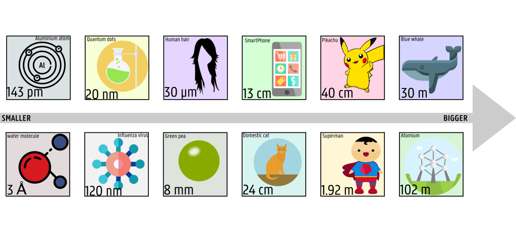
So what are nanomaterials? Any dictionary you open will tell you that it is something that has a size in the nanometre (notation: nm) range – and that a nanometre is equivalent to 10-9 m (or 1/1000000000 of a meter). Ok, so something small. But how small exactly? Let’s start by something quite familiar to us: a green pea, it has an average diameter of 8 mm (or 8×10⁻³ m), it fits in your hand easily, and it is visible with the naked eye ~ easy-peasy. Now, let’s try something familiar again but smaller: a hair. OK, depending on your type of hair, it might not always be exactly the same, but it will most definitively be in the tens of micrometer (μm) range – which is equivalent to 10-6 m (1/1000000 of a meter). A single hair you should still be able to hold between fingers, though you might need some contrast and better light to be able to see it with your eye. And you will definitively need an optical microscope to see it properly (to see its texture, all the different parts, the damaged end…). And after that, there is not much our own eye can see – without some help from special microscopes. So now, we will have to leave the tangible and continue to dive in scale. If we take something like a common influenza virus, then it is usually around hundreds of nanometre (nm). Ah! So is this a nanomaterial? We cannot see it and touch it (in the sense of feeling its presence on our skin), and it is in the size range of 10-9 m. Well, to be fair, it is still slightly too “big” to be qualified as a nanomaterial. At least, for people like us who work with nanomaterial in the range of tens of nanometres. Typically, some will defined the “actual” range of nanomaterials to be 1-20 nm, but some extent it up to at least 100 nm. It all depends on what you plan to do with it.
Wait, rewind a bit: aren’t nanomaterials just defined by their size – in the nanometre range, like we just learn and like their own name state? Well, of course size is important as a basic criterium for its definition, if your material is 2 mm, you will never convince anyone that it is a nanomaterial. But as stated earlier, some would defined their 50 nm-big material as a nano one, while others will argue that it is way too big for it! It all comes down to why we even bother going so small. Ah ~ now that is an interesting question. Why trying to scale down materials, that already exists most of the time, if that means they will be so small we will not be able to see and manipulate them without specialized (and costly!) equipment?
Scaling down a material has fascinating, counter-intuitive and downright weird effects on the characteristics and physics of a material.
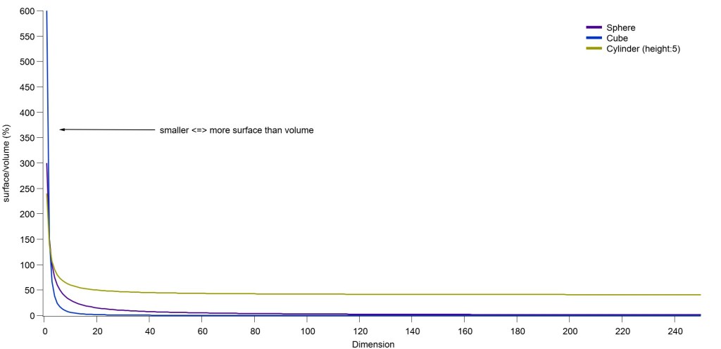
Let’s start with a counter-intuitive one: if you scale down something, you increase its surface area, compared to the total volume. Let’s take a simple example: a football ball. There are different sizes for different age group, we can take the biggest one, size 5 with a diameter of 22 cm. Then there is the smallest one of 14 cm diameter. We will have to do some simple maths, to determine their surface area: A=4πr2. And to determine their volume: V=4/3 πr3. With π the Pi number and r the radius (half of the diameter). So let’s do it: the size5 has a surface area of 1521 cm2 and a total volume of 5575 cm3, while the football size1 has a surface area of 616 cm2 and a total volume of 1437 cm3. mmh, well, it seems that I lied no? The smallest football size1 has a smaller surface area than the biggest football size5. What is going on? But I did not lie, what I stated was that when you go smaller, you increase the surface area – compared to its volume. So we need to do some more maths, this time to check this: do we have more “area” than volume for a smaller object? We can just check how much of “area” we have compared to volume, simply by dividing the surface area A by the total volume V: A/V. And to make it easier to interpret the results, we can multiply it by 100, and we obtain… percentage! So we will have an idea of how much area with have per total volume for the two different football sizes. OK, let’s do this. Let’s take football size5 (the biggest one): 1521/5575 x100= 27%. Now let’s try with the smallest football size1: 616/1437 x100= 43%. So what does that mean exactly? Well, we try to see how much “area” was in the volume of our balls. So if we have a lot of area, the percentage calculated will be large too – in other words, we will have much more “area” in the volume. And here it is: the smallest ball (football size1) has almost 50% (half) of itself is surface, while the biggest one (football size5) only has 30% (one third)! Counter-intuitive right? And this applies to all sizes and shapes – even to living beings. But why would that be interesting for us, scientists in our laboratories? Well, a lot of physics and phenomenon happens at the surface. After all, how can a virus enter a cell, without first interacting with its membrane? If you apply paint on a wall, only its surface will be coloured. When you jump in a pool, only the “surface” of the water splash. This is one of the reason it is interesting to scale down our everyday materials: we can increase their yields for a smaller amount of material (volume total). In this case, any material smaller than hundreds of nanometre would be called nanomaterials by their creators.
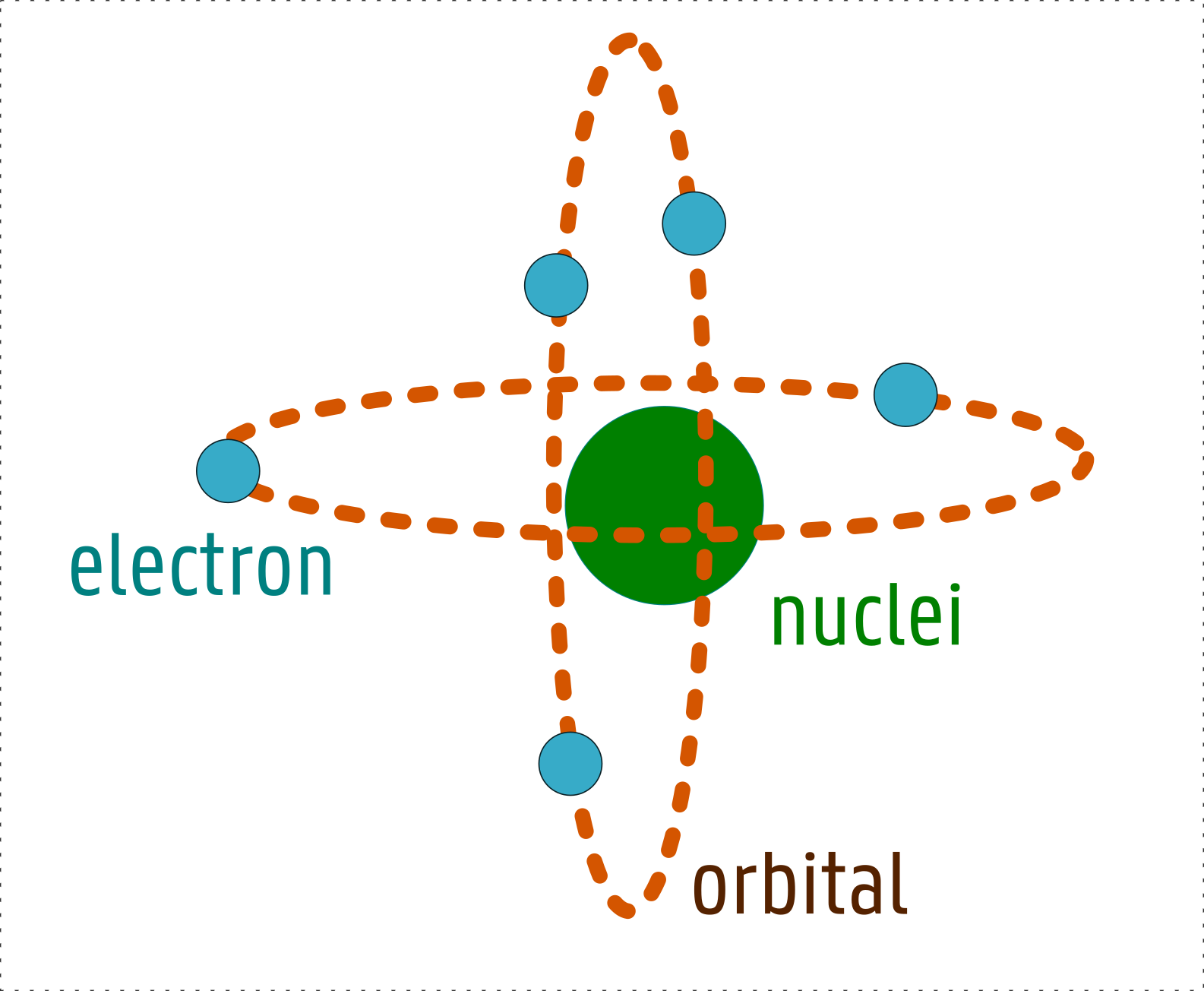
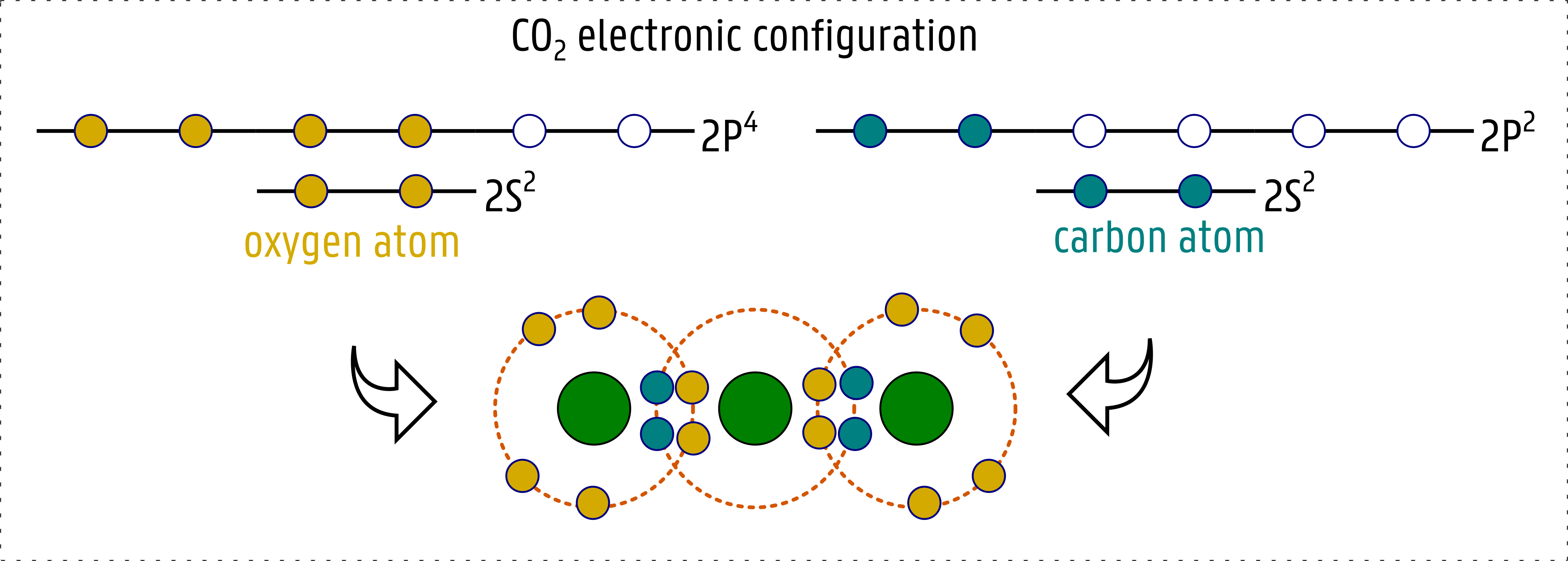
But why then be so finicky about the size range definition of nanomaterials? Well, if you want to use the materials’ particular weird physics that occurs only in the tenth of nanometre range, then a hundred nanometre material is not a nanomaterial at all (for you). See, it comes down to quantum physics – where all the classical physics kinda lead you astray. In the very small, classical physics is not the best tool to understand what’s happening. And this is because in our world (at our scale), we experience the cumulated/muted phenomena of all the small nano (and smaller!) world. Basically, classical physics is a summary, an average if you want, of all the quantum physics. It is also interesting that sometimes, some quantum physics can be experienced on our scale (yup, you read that right!). For instance, the photoelectric effect, which is basically the emission of electron (charged particles) from a material after absorbing light. The physics behind it are explained via quantum physics, and yet your TV remote control uses it to work! I will not make it a course on quantum physics. I just want to introduce a specific characteristic of nanomaterials – compared to their bulk (real-world size) one. When you make a nanomaterial, you have a very small amount of building blocks, compared to a bulk one: you can even count (with the help of computers) how many atoms you have in it. And this is why it gets interesting. When you have a single atom, you can represent it this way: a big centre (called the nuclei, composed of neutrons and protons) and a fixed number of negatively charged particles (called electrons) orbiting around (this is called the planetary model). It is only a visualization, it is more complex than that, but it gives a good grip on the concept. So here we have, the more mobile and volatile electrons turning around and around the nuclei, as they are attracted to the protons, which are positively charged. Now, if you go with the planetary system, you can also start thinking of the orbits, where do the electrons travel around the nuclei? And how many electrons can you make travel on the same trajectory? Well, all of this is determined by the nature itself of the electrons, and codified by quantum physics. The gist of it is as follows: electrons like protons, but they don’t like each other much. So you cannot put all the electrons you need (to make a neutral atom, you need the same amount of electrons and protons) on the same trajectory around the nuclei (in fact you can only put pairs depending on how large is your trajectory: 2,4,6…). So now you are in need of several orbits, with careful consideration on how they cross each-others and also remembering that, unlike planets, electrons can move all around the nuclei (in all directions). This is how we define electronic orbitals (with Fermi’s Golden Rule), where some electrons will be close to the nuclei, while some will be furthered and further away. What does it matter? Well, remember, the electrons like to be close to the protons (they are opposite charges), this is formalized as Coulomb force, and you can experience it in everyday life, as it is why you get sparks when you touch something (like a door handle). This force depends on how close the two charges are, so the closest they can be, the stronger their attraction. This give us two clues: the electrons in an atom will not be able to be as close to the nuclei as they want, they will have to settle for different orbitals & the electrons will not experience the same attraction depending on how far they are to the nuclei. And there. There is the source of all weird and quirky physics. But what of the nanomaterials, then? If you start adding atoms together, you can create for instance molecules: two hydrogen atoms associated with an oxygen atom, and voilà, a water molecule. You will still have all those atomic rules on how to organize the electrons around the nuclei, but now you will also need to arrange for the other electrons and nuclei! So you will start building new, slightly different, orbitals for all these electrons (which often do not stay attached to a particular nuclei). And let’s continue adding more and more atoms together. So that we have a cluster of atoms, with thousands of them. Now we start to see some averaging of all these orbits, and a “wholeness” of the object. And if you continue to add more atoms, at some point you will reach something of the size of tenths of nanometre: a nanomaterial. And the magic of the special orbitals, the difference in distance to the nuclei and so on, it will still be there! The nanomaterial will behave more or less like a giant atom. And its characteristics will inevitably depend on its size!


In summary: if you scale down enough to an everyday material, you can have more surface area to play with, and you will have some atomistic-like behaviour. What does that mean? It means that some very important characteristics of a bulk material can be enhanced/more efficient in your nanomaterial. And this is where the PCN group work on: to use the optoelectronic (light and electricity) properties of materials by scaling them down. Sometimes, you can also create/change characteristics of the material itself!
Our group work on two-dimensional nanomaterials: it means that they have one dimension (for instance, the width of the nano-object) that is small enough to be described with quantum physics, while the other two are slightly bigger and not as affected by quantum confinement (the size for which quantum physics apply). Specifically, we synthesize – meaning we cook with chemicals – nanoplatelets. Those are extremely thin (confined in the thickness) blocks of materials, with typical dimensions of: 10x30x2 nanometre. The thickness is small enough to be strongly confined (strong effect on the properties of the material), while the width is just at the limit (weakly confined) and the length is too large for quantum physics to apply. So what does that means? If you remember, we stated that for a nanomaterial, if it is small enough, it will have characteristics like a giant atom: the electrons will not be able to mix up as they want, and they will have to very strict orbitals (corresponding to their energy); and this is reflected if you confined (if you have a dimensions small enough) your material in three dimensions (0-D, yes confusing sorry). The 0-D nanomaterials are called nanoparticles and are the easiest structures to fabricate – as you can start with a “seed” of few atoms attached together and start assembling them together with some extra energy (usually by heating). Since they will show characteristics similar to that of actual atoms, they will have very strict electronic orbitals, which in turn means that they will display atom-like response to stimuli. What does that mean? Remember the planetary model of the atom: nuclei more or less fixed and positive, surrounded by fast moving negative electrons on specific orbitals, with a limited number of electrons allowed on the same orbital. Well, you have to imagine that these “allowed” orbitals that are filled with electrons, are not the only ones, there are empty ones available above the full ones. We state that the atom is at rest when all the electrons are at the lowest (closest to the nuclei) orbitals, because then they have the lowest energy possible (they feel the attraction of the nuclei strongly, and remember, they want to be with the protons in the nuclei). But it is possible – and very banal in fact – to give extra energy to an electron, so much that it changes orbital! To do so, you can simply shine some light on the atom, if you are lucky, you will have just the right type of energy to give to the electron. Why the right type? Why not just shine any light and poof the electron gets excited (has extra energy)? Well, remember that the electrons are not happy to be together, so much so that if their orbitals is not big enough, they can only be two on it (the smallest orbital, called s-orbital, shape like a sphere). And so they have orbitals that are separated both physically in space – but also, and more importantly, in energy! The closer the electron is from the nuclei, the most energy it needs to change orbital to one further away. And this is why we state that quantum physics apply: the energy of the things are quantized. This is why you need the right type of light to give energy to an electron in an atom: only light that have the energy difference between the two orbitals will be able to make the electron change orbital (get excited). Of course, it only makes sense if you remember that light has a dual nature: it behaves like a wave (ripples on the water surface, sound waves in the air) but can also be described as a collection of particles (called photons). And since it is weird and bizarre, you can be sure that quantum physics apply here too: the photons are quantized, each will have a specific energy. And since light can also be described as a wave, you can link the photon’s energy with the wave basic physical characteristic: the wavelength (peak to peak distance). A bit confusing, hum? Do not despair, this is the basics you need to know to understand why nanomaterials are interesting. So we have electrons in atoms that can only absorb certain photons that have the right energy for them to change orbitals. Well, in a 0-D nanomaterial, something similar happens! The atoms are all put together, so there is a bit of mixing of all their electrons, and so if you imagine all the electrons together, they will arrange themselves similarly to the electrons in the atom: the only difference this time is that they are more options. Why more options? Well, if you think of a floor to fill up with tiles, if you have a very small room, you will have no place to make a picture with the different tiles, compared say to the hallway of a big reception room. This is the same idea, you will have much more electrons to “play” with, to arrange and organize in orbitals. That is how the nanoparticles are similar to atoms: you will need specific (quantized) energy to excite electrons and make them change orbitals. OK, that is cool, but why would that be interesting exactly? Because the cool stuff about excited electrons, is that they do not really can stay excited indefinitely, they will lose energy and go back to their “rest:” orbital. And to lose energy… they emit a photon with the exact energy they need to lose!! And of course, it happens in nanomaterials too. In nanomaterials, you have a bit more wiggle room, remember, you have more options in organizing your electrons in orbitals. The more electrons (aka the more atoms) you had, the more orbitals you make, to a point where they are so many choices that we say there is a continuum (in bulk materials). Anyway, if you have wiggle room, you can absorb several photons with different energy – and emit back photons at the same energy! So now we have materials that can absorb some light and give back a very uniform colour – an emitter. This way, you can create light-emitting diodes (LEDs), and a lot of other cool things (like taking sunlight and converting it to a specific light that is absorbed by a solar cell). So why do we bother making 2-D nanomaterials? Well, when you confine your electrons in only one dimension, you have a mix of very strict orbitals with the continuum of the bulk: you have a lot of possible light absorption, but you still only emit one colour! To add to their coolness, the nanoplatelets will emit 80% of all their light from their plane (so 20% on the side), which means that you will have a very directional light emission. They also have another characteristic which makes them potential lasing material (it is a tad complicated matter). A laser is a very coherent (the light emitted is very “pure” in colour) and powerful. Existing laser are bulky and expensive to make, so the idea is to use the nanoplatelets to design a laser.
Why using nanoplatelets (NPLs) better? Because they are synthesized: they are cooked with chemicals. It is called bench-fabrication (or sometimes wet-fabrication) and it is easier to scale up, cheaper (than physical deposition, where you build atom by atom the material by usually evaporating a source of each atom you need) and at low temperatures (compared to bulk material which start above 250 °C at minimum, for amorphous Silicon for instance). So, how does one synthesize NPLs? And what are they made of anyway? We use what is called semiconductor materials, meaning materials that can only slightly conduct electricity (in between a metal, like copper, and an insulator, like wood). A very well-known semiconductor material is Silicon, as it is used in a lot of electronic applications (as well as a typical solar-cell building material). Particularly, we use II-VI semiconductor, meaning we mix two different atoms to create a new material with a mixture of both characteristics. For instance, mixing a metal (cadmium) with a chalcogen (selenium), makes a semiconductor CdSe. Other example of II-VI semiconductors we make at PCN: CdTe, ZnS, CdS, InP, ZnSe… For now, we are trying to reduce the use of the metal cadmium as it is not really abundant and rather toxic – compared to manganese (Mn), zinc (Zn) and calcium (Ca). Let’s go through a typical recipe to create a thin nanoplatelet of CdSe anyway, but do not make it without the proper safety equipment!
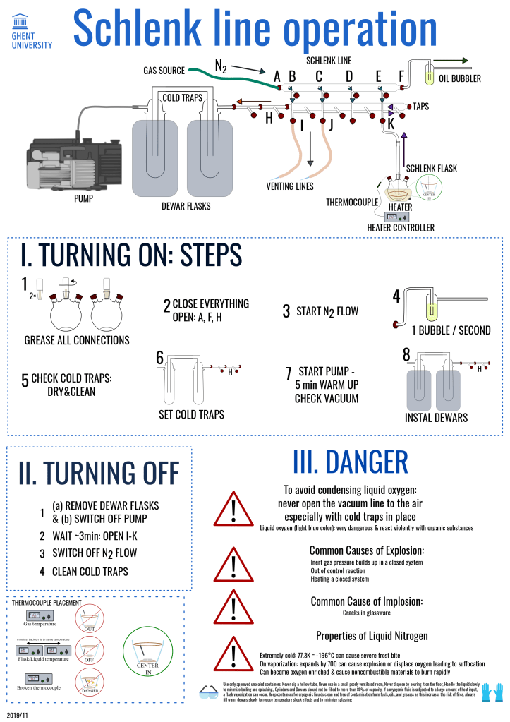
Let’s synthesize 4.5 monolayer thick CdSe NPL. For this recipe you will need for equipment:
- a Schlenck line: to have both gas purge and vacuum
- a vacuum pump & a N2 gas tank
- a heating mantle, thermocouple & a PID heating system: to set and control the temperature
- a 50 mL three-necked flask & condenser: where the reaction takes place
- a magnetic stirrer and a magnetic rod: to help mix all the chemicals together
- a weighting scale (precise to the 0.001g) and various spatulas, syringes…
And for original ingredients:
- 1-ODE (octadecene): 25 mL
- Cd(Act)2-dihydrate (cadmium acetate): 88 mg
- Se (selenium) powder: 24 mg
- Cd(Ole)2 (cadmium oleate): 550 mg
- Cd(My)2 (cadmium myristate): 340 mg
Follow the following steps carefully, assuring yourself of the purity of your chemicals and the cleanliness of your equipment:
- Weight in the dry flask the cadmium myristate & selenium powders
- In separate vials, weight the cadmium acetate powder & the cadmium oleate wax
- Set the flask on the heating mantle, add the condenser (do not forget to grease the connections)
- Add the octadecene, try to wash the left-over powder from the neck sides
- Add the magnetic rod, set the magnetic stirrer to around 600 RPM
- Flush the equipment with N2 for a few minutes, then seal the flask’s necks
- Set the thermocouple on the underbelly of the flask
- Close the N2 flow, start heating to 90 °C, vacuuming for at least 1h
Once all the water has bubble out under the vacuum in the system, the reaction to create NPL can take place:
- Stop vacuuming and open the N2 flow again
- Set the vial of cadmium oleate on a heating plate, set to 90 °C
- Stop the heating mantle, move the thermocouple inside the flask (it should be in the liquid)
- Set the heating temperature to 240 °C, watch as the colour of the liquid goes from white translucent to yellow, orange then red
- Once the temperature of the liquid mixture reach 240 °C, introduce rapidly the cadmium acetate powder, you can stir manually by shaking the flask
- Start a countdown watch once the temperature reach 240 °C again, controlling the reaction time control the width/length of the NPL, around 9 min growth gives a 10×30 nm
- Once the reaction time has been reach, remove the heating mantle and inject the liquified cadmium oleate
- A cooling bath can also be used to cool down faster the solution, which should be dark red
Now you have a nice batch of… NPLs and quantum dots! What? Really? Unfortunately, the nanoparticles are much more thermodynamically favourable – in less gibberish, it is easier to make round-ish objects than other deformed shapes, as you need to control the direction of growth. But not all is lost, a simple play with some solvents (add some acetonitrile, hexane and isopropanol), make a wild ride in the centrifuge, and hop only NPLs remain. I know, I know, sound complicated. But really, not that difficult to make, you just need the proper equipment of course. And the cool stuff with all this cooking, is that you can change small steps and obtain different thicknesses of the same shape, or you can add another step and coat your NPL with something else (often we have CdSe/CdS layers). Chemistry is extremely versatile, and often careful preparation need to be done beforehand while trying to make a new synthesis (making new material, shape…), often with a design of experiments.

Schlenck line in fume hood 
Synthesis of 4.5ML CdSe NPL 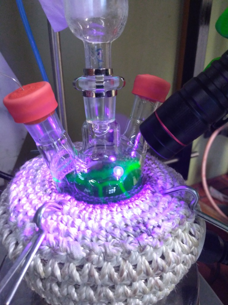
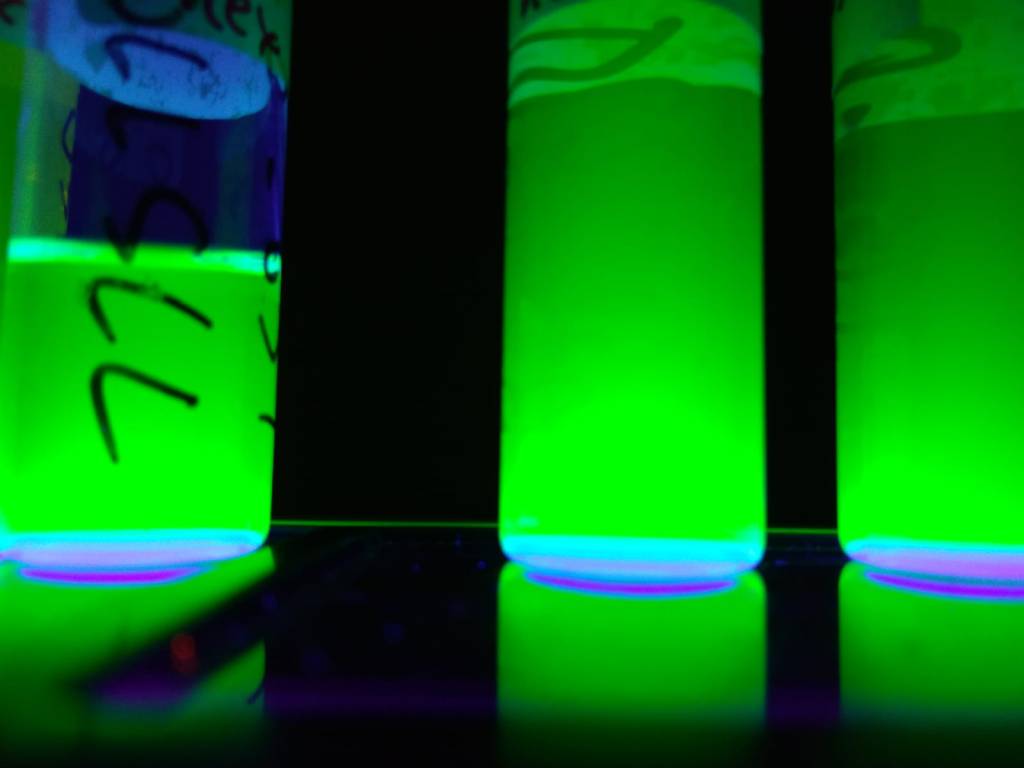
Green emission of 4.5ML CdSe NPL under ultra-violet light 
Vials of different NPLs solutions
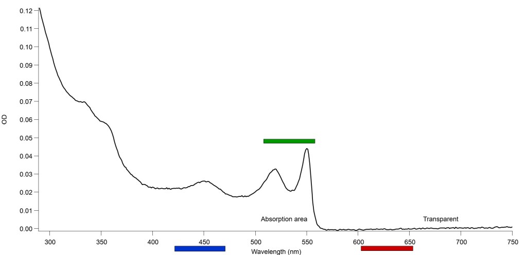
It is fun to characterize the nanomaterials, you can use an electron microscope (TEM JEM-1010 from JEOL) to determine their dimensions, optical spectroscopy to verify their absorption (we use a Lambda 365 from Perkin Elmer) and emission (we use a LED laser combined with a spectrometer from Avantes). Summarily, an electron microscope uses electrons to make “images” of an object (it has to be extremely thin), making a contrast between the background (usually a grid with carbon sheets) and the nano-objects on it. A spectrophotometer will shine light through a solution and measure how much has disappeared, at each wavelength (each colour), which can be displayed in a graphical form of the optical density (OD, how much light is absorbed by the material) as a function of wavelength. And in the emission spectroscopy, the light also shined on the solution, but this time, it is light emitted by the solution that is measured (for instance, you shine on one side and measure at a 90-degree angle). This way, you can plot the intensity of the light measured (the units depends on your equipment or the analysis you make) as a function of wavelength (colour).


To be able to use the NPLs, we are trying to deposit them in an ordered fashion, on functional substrates. For instance, if you want a laser, you will need the emitting layer (the NPL one) sandwiched between two reflective substrates (that will reflect the emitted colour). And since you want it to be efficient and with the least amount of loss (when you will put electric power in for instance), the NPL need to be all oriented the same way and in a neat pile! To realize this we are working on assembling the NPL together on the surface of a liquid, to then pick them up with a special stamp (a jellylike material that does not like water), to, well, stamp the assembled NPLs on the substrate. Let’s hope it works!
